4H 6inch SiC Epitaxial Wafer 100μm/200μm/300μm for Ultra-High Voltage (UHV) MOS Device
The 4H-SiC epitaxial wafer is a core material for carbon disulfide (SiC) power devices, fabricated on a 4H-SiC single-crystal substrate via chemical vapor deposition (CVD). Its unique crystal structure and electrical characteristics make it an ideal substrate for ultra-high voltage (UHV, >10 kV) metal-oxide-semiconductor field-effect transistors (MOSFETs), junction barrier Schottky diodes (JBS), and other power devices. This product offers three epitaxial layer thicknesses (100μm, 200μm, 300μm) to address applications ranging from low-voltage to UHV scenarios, suitable for new energy vehicles (NEVs), industrial power systems, and smart grid technologies.
SiC epitaxial wafer Characteristic

1. High Breakdown Voltage & Low On-Resistance
- Achieves balanced breakdown voltage (BV) and specific on-resistance (R<sub>sp</sub>) via deep doping pillar structures (alternating n-type and p-type columns). For example, 5 kV-class SJ MOSFETs exhibit R<sub>sp</sub> as low as 9.5 mΩ·cm² at room temperature, rising to 25 mΩ·cm² at 200°C.
- Adjustable epitaxial layer thickness and doping concentration (e.g., 100μm layer for 3.3 kV devices, 300μm layer supporting >15 kV applications).
2. Exceptional Thermal Stability & Reliability
- Leverages high thermal conductivity (4.9 W/cm·K) and wide bandgap (3.2 eV) to operate stably above 200°C, minimizing thermal management complexity.
- Employs ultra-high energy ion implantation (UHEI) (up to 20 MeV) to reduce lattice damage, combined with 1700°C annealing to repair defects, achieving leakage current density < 0.1 mA/cm².
3. Low Defect Density & High Uniformity
- Optimized growth parameters (C/Si ratio, HCl doping strategy) yield surface roughness (RMS) of 0.4–0.8 nm and macro-defect density < 1 cm⁻².
- Doping uniformity (CV testing) ensures standard deviation < 15%, guaranteeing batch consistency.
4. Compatibility with Advanced Fabrication Processes
- Supports trench filling and deep doping pillar architectures, enabling lateral depletion designs for UHV MOSFETs with breakdown voltages exceeding 20 kV.
4H-SiC Epitaxial Wafer Applications
1.Ultra-High Voltage Power Devices
- New Energy Vehicles (NEVs): Main drive inverters and onboard chargers (OBC) for 800V platforms, enhancing efficiency by 10–15% and enabling fast charging.
- Industrial Power Systems: High-frequency switching (MHz range) in photovoltaic inverters and solid-state transformers (SSTs), reducing losses by >30%.
2.Smart Grids & Energy Storage
- Grid-forming energy storage PCS for weak-grid stabilization.
- High-voltage DC transmission (HVDC) and smart distribution equipment, achieving >99% energy conversion efficiency.
3.Rail Transit & Aerospace
- Traction inverters and auxiliary power systems for extreme temperatures (-60°C to 200°C) and vibration resistance.
4.Research & High-Tech Manufacturing
- Core material for ultra-heavy element (e.g., Nh) detectors, enabling high-temperature (300°C) α-particle detection with energy resolution < 3%.


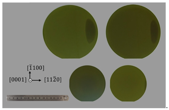
4H-SiC Epitaxial Wafer parameters
| Parameter | Specification / Value |
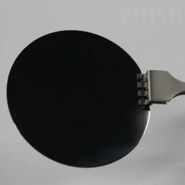
| Size | 6 inch |
| Material | 4H-SiC |
| Conductivity Type | N-type (doped with Nitrogen) |
| Resistivity | ANY |
| Off-Axis Angle | 4°±0.5° off (typically toward [11-20] direction) |
| Crystal Orientation | (0001) Si-face |
| Thickness | 200-300 um |
| Surface Finish Front | CMP polished (epi-ready) |
| Surface Finish Back | lapped or polished (fastest option) |
| TTV | ≤ 10 µm |
| BOW/Warp | ≤ 20 µm |
| Packaging | vacuum sealed |
| QTY | 5 pcs |
More samples of SiC Wafers

*We accept customized one, please feel free to contact us about your requirements.
Recommended SiC Products
SiC Epi Wafer FAQ
1. Q: What is the typical thickness range for 6-inch 4H-SiC epitaxial wafers?
A: The typical thickness ranges from 100–500 μm to support ultra-high-voltage (≥10 kV) MOSFET applications, balancing breakdown voltage and thermal management.
2. Q: What industries use 6-inch 4H-SiC epitaxial wafers?
A: They are critical for smart grids, EV inverters, industrial power systems, and aerospace, enabling high efficiency and reliability in extreme conditions.
Tags: #6inch, #Custom, #4H-SiC Epitaxial Wafer, #4H-N Type, #100μm/200μm/300μm, #Ultra-High Voltage (UHV), #MOS Device, #SiC Crystal, #Silicon Carbide Substrate, #100-500μm


